Importance of Signal Integrity in PCB Design
NOTE: This article/blog is Copyright TronicsZone. It cannot be reproduced without prior written approval.
Introduction
High-speed digital circuit design is on the rise in recent times. With the frequency of the clock used in PCB increasing and the data rates of the communication protocols increasing, PCB has become a structure built to deliver supreme performance. Taking such high performance metrics into consideration, it is important for a designer to plan high-speed interconnects and select board material with desired characteristics.
The success of signal-integrity in a PCB design depends on handling bottlenecks such as reflection, crosstalk, delay, and impedance matching – which are routinely done by us here at Tronicszone. These problems are the result of increasing data rates at the Input/output and memory interfaces, and due to the high-speed transceiver technologies that are embedded into FPGAs and PCBs. This article discusses various reasons that affect the signal integrity in a PCB design and the good design practices used to overcome these shortcomings.

Signal Integrity in PCB Design
Signal integrity of a device is ensured by designing the wires and interconnects so that they carry correct and uncorrupted data. Analog signal integrity was a challenge to design but digital systems are comparatively easier to design. Still, digital systems are also susceptible to noise. The size of devices are reducing with technology and so the interconnects are placed close together. This makes the designer’s job more critical during the initial stages of a PCB.
It is important to follow good practices and check for integrity right from the simulation stage itself. Software like Cadance (SI) analysis, Ansys (SI) analysis provide an insight on the design requirements. It is better to focus on signal integrity during simulation and floor planning stage, since not much can be done after physically designing the PCB.
Problems Causing Signal Loss in PCB
The most important issues that affect the quality of signal transmission in a PCB are transmission line effects, impedance mismatch, high-speed switching characteristics, board material loss, and crosstalk. These issues and their remedies will be discussed in detail.
Transmission Line Effects on Signal Integrity
Transmission lines are defined as a conductive medium or connection between the transmitter and a receiver, which is capable of carrying a signal. At high-speed digital signal transmission, even the shortest passive printed circuit board (PCB) tracks are affected by the transmission line effects. At low frequencies, the impedance of a transmission line is only resistive. Hence the characteristic impedance of the transmission line can be expressed at low frequencies as
Z0 = R = V/I (Ohm)
At high frequencies, the AC circuit characteristics become dominant in the transmission line and this is due to the introduction of capacitive and inductive reactance. The reactance is the complex part of impedance. So at high frequencies the impedance of the transmission line can be realized as
Z0 = R +jX
X = XL + XC
Where XL is inductive reactance which is directly proportional to frequency and XC is capacitive reactance which is indirectly proportional to frequency.
Hence to overcome transmission line effects, the designer’s ideal choice is to maintain the characteristic impedance of the transmission line the same along the length of the line. In case of any discontinuities such as open or closed circuit, the signal is lost in the form of radiation or reflection. The factors affecting the resistance and reactance of the transmission lines in PCB are line thickness, dielectric constant of the board, distance between the line and the ground plane. So by playing around with any of these parameters the designer has to maintain the impedance same along the length of the transmission line.
Impedance Matching Effect on Signal Integrity
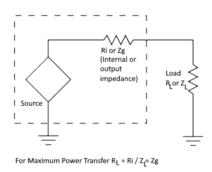
A similar scenario to the transmission line effects is the impedance matching. For maximum coupling of signal power between two ports, the load impedance of the output port has to the equal to the characteristic impedance or the internal impedance of the circuit.

When there is a mismatch between these impedances not all of the signal power is coupled, but a part of the signal is reflected back in the transmission line. This causes standing wave in the transmission line leading to overshoot, undershoot, stair step waveforms and ringing. These conditions affect signal integrity vastly.
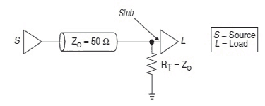
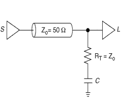
Impedance mismatching problems can be eliminated by careful selection of medium and by termination schemes. The selection of termination scheme depends on the application and requirement. A simple parallel resistor to the ground (simple parallel termination) or a complex RC termination which is a low pass filter used to remove low frequency noise and to pass the high frequencies can be used. Stub matching is also a solution to match the impedance correctly.
 Simple Parallel Termination

RC Termination
Board Material Effects on Signal Integrity
Choice of PCB materials affect the signal transmission. Signal losses occur due to attenuation. Dielectric material is an indispensable material in PCB. At high frequencies the molecules of the dielectric medium are excited. Excited molecules absorb some of the signal energy, leading to signal loss. This is termed as dielectric absorption. This can be reduced by careful selection of the dielectric material of the PCB.
Another issue in transmitting signals via conducting wires is the skin effect. At very high frequencies the signal power tends to travel on the surface of the conductor alone. This is Skin effect. Due to this the effective conductive area is reduced. Any discontinuities on the surface of the conductor will lead to signal attenuation. Signals traveling on the surface of the conductor results in self-inductance which results in increased inductive reactance. Skin effect can be minimized by increasing the width of the conducting surface.
Pre-Emphasis and receiver equalization techniques can also be used to reverse attenuation loss. In pre-emphasis, the high-frequency signal components are amplified and transmitted to withstand the signal attenuation and in receiver equalization, low frequency signals are specifically attenuated at the receiver end using dedicated circuit to compensate for the line losses.
Effects of Crosstalk on Signal Integrity
Crosstalk in a PCB is due to mutual inductance and mutual capacitance. A transmission line carrying a signal power develops a magnetic field around it. When parallel lines are used close together in a PCB, a magnetic coupling occurs between the two lines, resulting in the coupling of the signal energy. This is termed as crosstalk. Mutual inductance happens when the current in one line couples a magnetic field in the adjacent line and the inductance varies with varying current on the original line. Mutual capacitance occurs due to coupling of electric filed among adjacent lines and is proportional to the rate of change of voltage at the signal driver end. Crosstalk damages the overall signal quality. Following are a few considerations to be followed during design to minimize crosstalk.
- The signal lines are placed apart such that the distance between two trace lines is not less than three times the width of the trace. This is 3W principle. This will help to overcome 70% of electrical field coupling.
- Proper impedance matching will eliminate reflection and thereby help in reducing crosstalk
- The traces are maintained as close as possible to the ground plane. This helps in coupling the signal in the transmission line tightly to the ground plane and decouple it from adjacent signals traces.
- Orthogonality shall be maintained between traces on different layers while routing. Different routing techniques for different frequencies can be done.
- Long parallel run of signal traces shall be minimized.
Effect of High-Speed Switching on Signal integrity
Simultaneous high-speed switching can impact the signal integrity. When a high number of outputs in a PCB switches from logic high to low, the charges accumulated in the load capacitors are coupled into the device. This results in high transient current into the device as the load capacitors discharge. This current is coupled to the ground and hence a low voltage signal is setup between the ground and the device board. This is termed as ground bounce. This ground bounce will result in wrong data being provided at the output terminals (always high).
Dedicated high-speed I/O pins, dedicated ground pin usage can minimize ground bounce. Proper grounding and minimizing simultaneous switching can improve the signal integrity.
General Precautions in PCB Design
Some of the general precautions that shall be followed during the design of a PCB are discussed in this section
- Right-angled traces are source of radiation and signal loss at high frequencies. Instead, a 45-degree bend or a round bend are preferred as routing bends.
- High-speed and high-frequency signals are separated from low frequency signals. Especially clock signal can be routed separately. Similarly, analog and digital signal routing shall be made separate.
- Vias are essential in PCB. But via result in additional inductance and capacitance. They also result in characteristic impedance changes, hence utmost care on all underlying conditions should be taken into consideration while designing vias.
- For high-frequency applications multilayer PCB with buried ground and power supply planes are preferred.
- Laminate material such as FR-4 or Rogers RO4350 are preferred. For 2.5-3 GHz range FR-4 delivers best results and Rogers RO4350 is preferred for higher frequencies.
- Signal integrity is also affected by Electromagnetic interference. Refer EMI/EMC for more details.
Conclusion
The reliability of a PCB depends on its signal integrity. High frequency of operation and the need to minimize the size of the device are the two of the most important requirements in current PCB designs. As discussed in this article, when it comes to signal integrity, following good practices in the initial stages of planning will help a lot than planning it during physical design. At TronicsZone utmost care is given by our design engineers to when it comes to signal integrity. Robustness and Reliability is our motto.
NOTE: This article/blog is Copyright TronicsZone. It cannot be reproduced without prior written approval.

 TronicsZone